Logo
Apparel & Fashion

Description

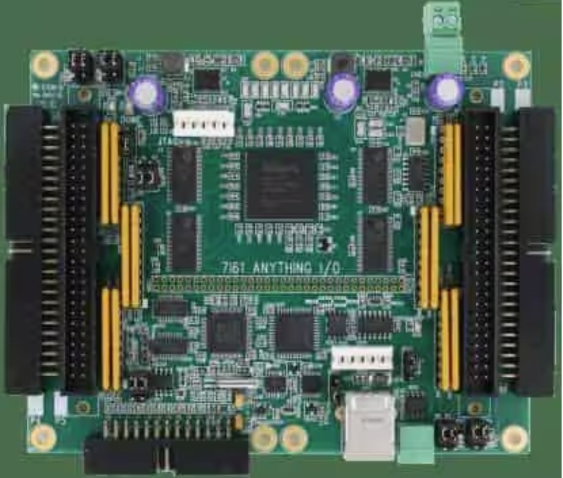
This circuit board layout service translates electronic circuit diagrams into high-density physical board designs. Engineering specialists assign exact component footprints, establish board mechanical boundaries, and route interconnection traces while preventing electrical noise interference. The routing process accounts for voltage isolation gaps, power distribution stability, and thermal dissipation needs across multiple copper layers. By running strict Design Rule Checks (DRC) against the original schematic netlist, potential trace shorts, unrouted connections, and manufacturing clearance violations are detected and resolved early. The completed layout yields standard fabrication packages containing vector graphics, drill patterns, and assembly placement coordinates for automated mass production.

Specifications

Key Attributes
Core FunctionSchematic to Board CAD Layout Conversion
Deliverable PackageExtended Gerber (RS-274X/ODB++), NC Drill, BOM, Pick-and-Place
CAD Tool SupportAltium Designer, KiCad, OrCAD, PADS, Cadence
Layer Range1 to 28+ Multi-Layer Boards
Trace IsolationHigh-Voltage Creepage & Clearance Checks
Signal integrityControlled Impedance, Differential Pair Matching
Manufacturing StandardIPC-2221 / IPC-A-600 / IPC-A-610
Additional Information
Country of OriginIndia

Application

Converts analog and digital circuit schematics into physical board manufacturing designs.

Routes compact double-sided board layouts for commercial LED lighting drivers.

Organizes high-density component layouts for consumer smart home controllers.

Optimizes trace geometry for noise-sensitive audio processing and amplification gear.

Designs multi-layer layouts for industrial sensor interfaces and power monitors.
Company Profile

Cosmic
Cosmic, Tamil Nadu
TruBasic
0
ManufacturerService Provider
Frequently Asked Questions
1
What primary information is needed to perform a circuit board layout?

A complete schematic file, netlist, bill of materials (BOM), and mechanical drawing defining the board boundary are required.

2
How does the layout service prevent interference between high-speed and analog signals?

Designers implement physical trace separation, ground plane isolation, guard traces, and orthogonal layer routing to eliminate cross-talk.

3
Are component footprints checked against actual physical parts?

Yes, footprints are verified against manufacturer datasheets and IPC-7351 3D CAD dimensions to ensure proper land pattern fit.

4
What standard outputs are provided for board fabrication?

The service generates Extended Gerber (RS-274X) or ODB++ files, NC drill data, fabrication notes, and assembly drawings.

5
How is thermal dissipation handled during the layout process?

Engineers place thermal copper pours, heavy ground planes, and thermal via arrays beneath heat-generating components to distribute thermal energy.

Circuit Board Layout Services

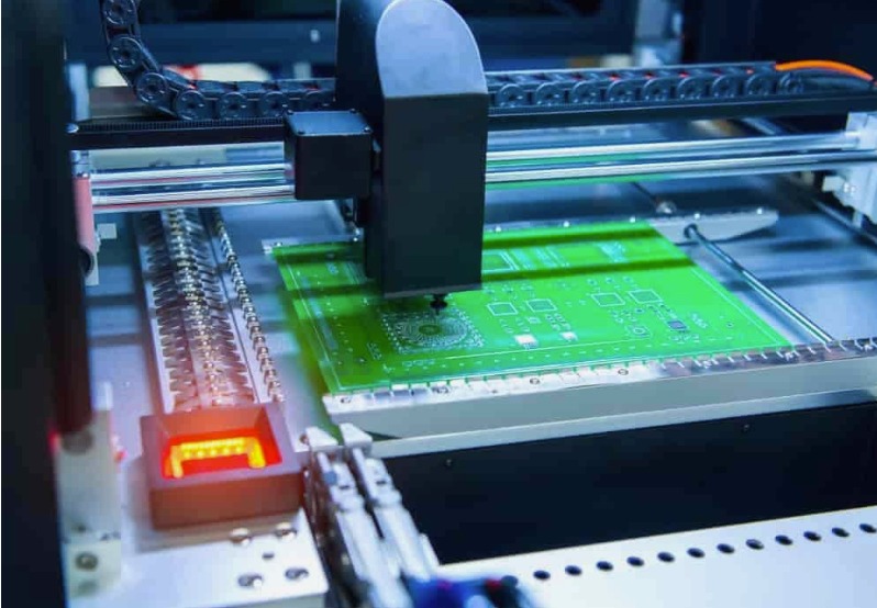
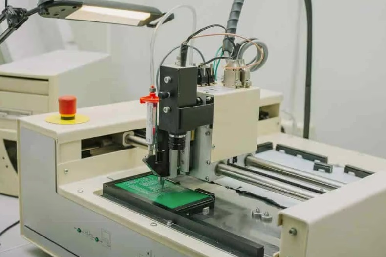
Circuit Board Layout Services specialize in converting proven electronic schematics into precise, defect-free circuit board conductor patterns ready for fabrication. This service manages track routing, component footprint mapping, and layer allocation to ensure optimal electrical continuity and manufacturability.

Min. Order Quantity: 1 piece

Shipping

Shipping fee and delivery date to be negotiated. Contact supplier now for more details.

Cosmic
TruBasic
Tamil Nadu, India
Manufacturer

More Products From Supplier