Logo
Apparel & Fashion

Description

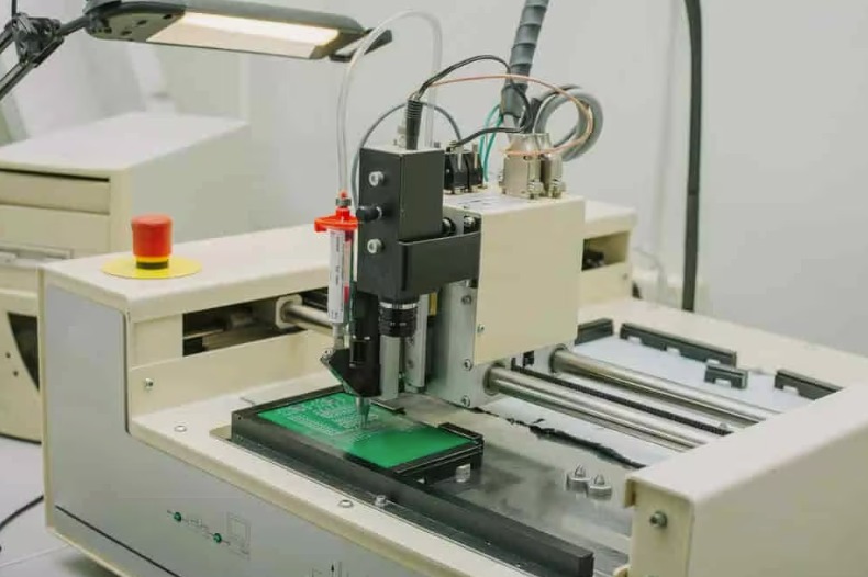
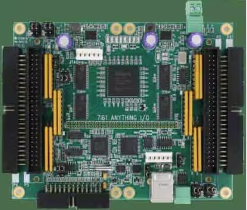
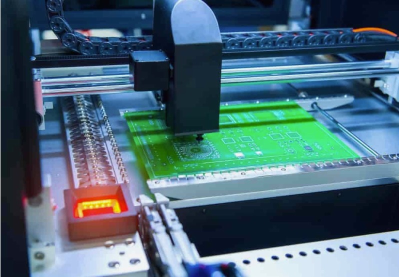
This PCB layout service transforms conceptual electronic schematics into fully optimized, production-ready printed circuit board designs. Utilizing advanced CAD tools, engineering teams precisely position surface-mount and through-hole components to maximize space efficiency while minimizing signal degradation. The layout process strictly adheres to Design for Manufacturability (DFM) and Design for Assembly (DFA) rules, eliminating costly production re-spins and yield failures. Special attention is given to high-speed signal routing, power distribution network balance, thermal dissipation paths, and electromagnetic compatibility (EMC) isolation. Upon completion, customers receive complete manufacturing packages containing Gerber files, assembly drawings, bill of materials cross-references, and drill files necessary for seamless factory production.

Specifications

Key Attributes
Service TypePCB Layout / CAD Routing
Deliverable FilesGerber (RS-274X/ODB++), NC Drill, BOM, Pick & Place
Supported Design ToolsAltium Designer, KiCad, Cadence Allegro, Eagle
Layer Count CapabilitySingle Layer to 32+ Layers
Board TechnologyRigid, Rigid-Flex, Flexible, High-Density Interconnect (HDI)
Signal Integrity FeaturesImpedance Matching, Differential Pairs, Length Tuning
Additional Information
Country of OriginIndia

Application

Routes high-density multi-layer circuit boards for compact consumer mobile devices.

Designs noise-isolated layouts for sensitive medical monitoring and diagnostic equipment.

Creates ruggedized power electronics layouts for automotive and electric vehicle controllers.

Optimizes high-frequency RF circuit layouts for wireless communication and IoT modules.

Converts legacy analog circuit designs into modern surface-mount technology board layouts.
Company Profile

Cosmic
Cosmic, Tamil Nadu
TruBasic
0
ManufacturerService Provider
Frequently Asked Questions
1
What primary inputs are required to start a PCB layout service project?

A complete schematic diagram, netlist, component bill of materials (BOM), and mechanical enclosure dimensions are required.

2
What design files are delivered upon completion of the layout service?

Deliverables include Gerber files, NC drill files, fabrication drawings, pick-and-place files, 3D STEP models, and BOMs.

3
How does DFM (Design for Manufacturing) checking benefit the project?

DFM checks ensure traces, hole sizes, and component spacings match manufacturing tolerances, preventing costly fabrication errors.

4
Can the layout service handle high-speed and differential pair routing?

Yes, design engineers configure impedance control, length matching, and cross-talk mitigation for high-speed signals.

5
What EDA CAD tools are commonly supported for PCB layout?

Layouts are typically developed using Altium Designer, Cadence Allegro, Mentor Graphics PADS, OrCAD, or KiCad.

PCB Layout Services

PCB Layout Services convert electronic circuit schematics into physical, manufacturable printed circuit board designs. This process involves component placement, copper trace routing, signal integrity management, and generating complete manufacturing file packages for board fabrication and assembly.

Min. Order Quantity: 1 piece

Shipping

Shipping fee and delivery date to be negotiated. Contact supplier now for more details.

Cosmic
TruBasic
Tamil Nadu, India
Manufacturer

More Products From Supplier