IN
IN₹
Apparel & Fashion
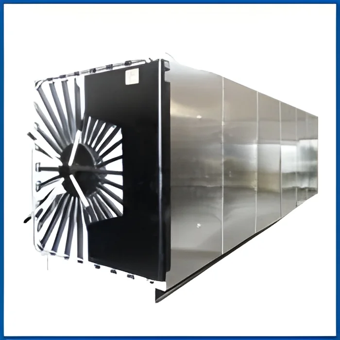
Description
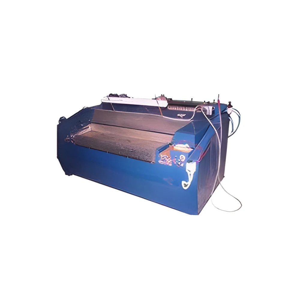
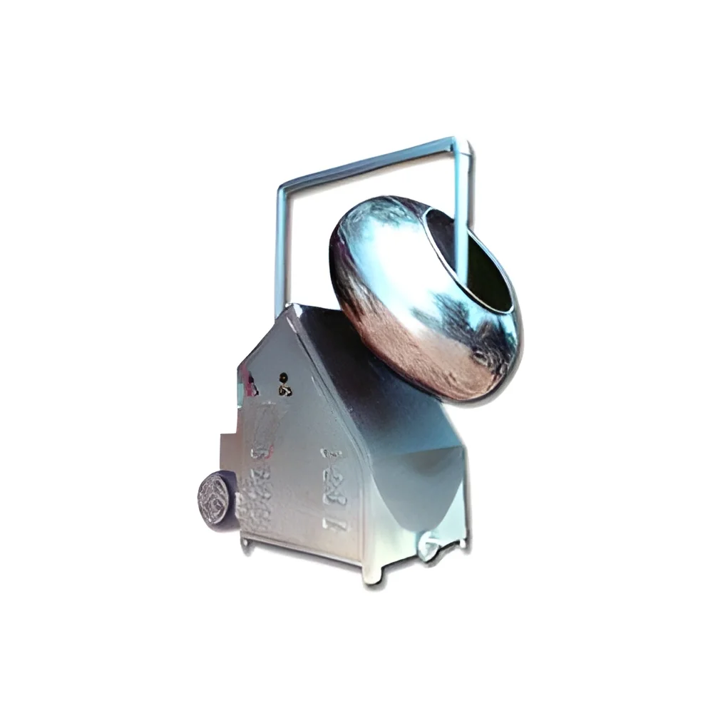
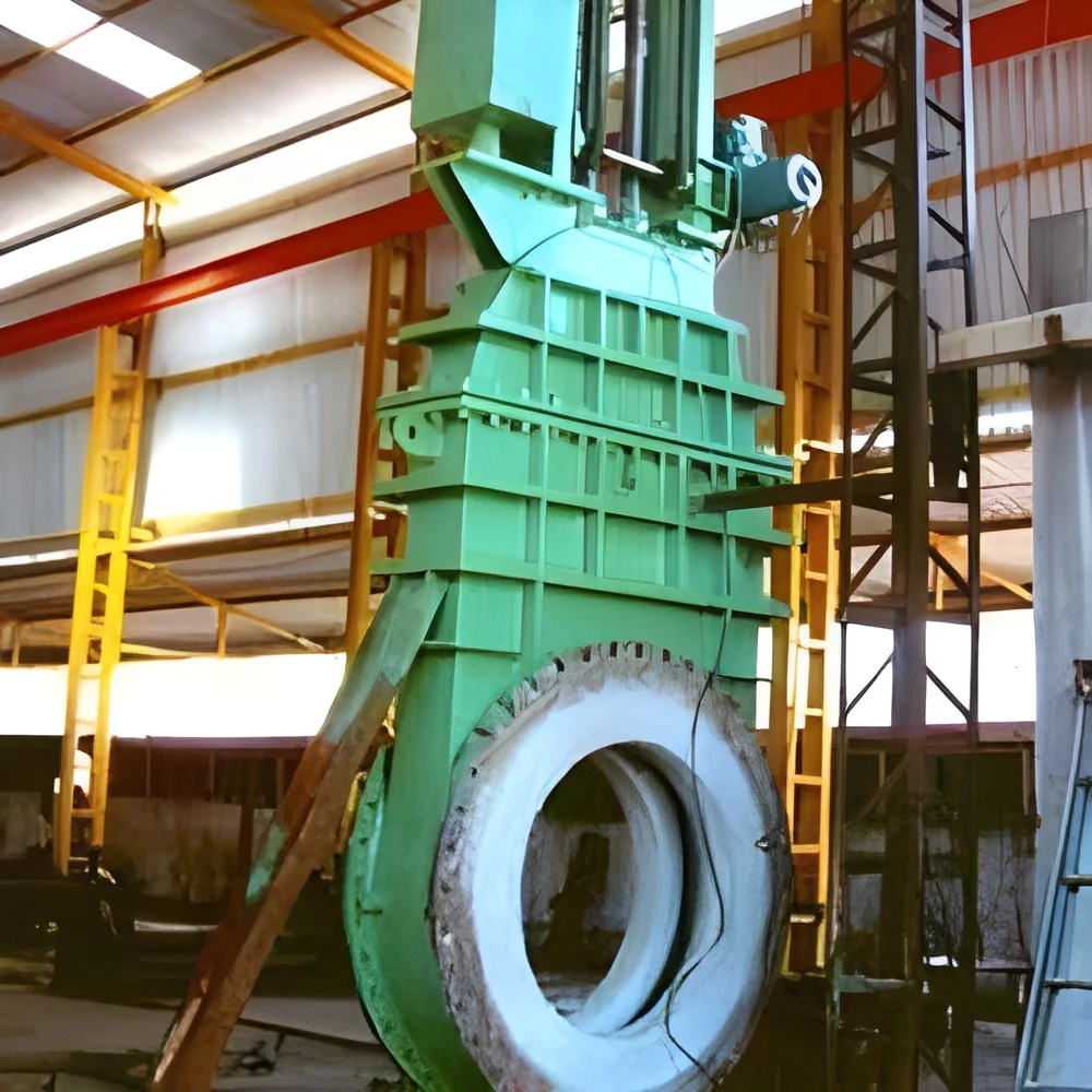
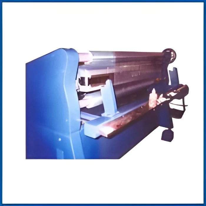
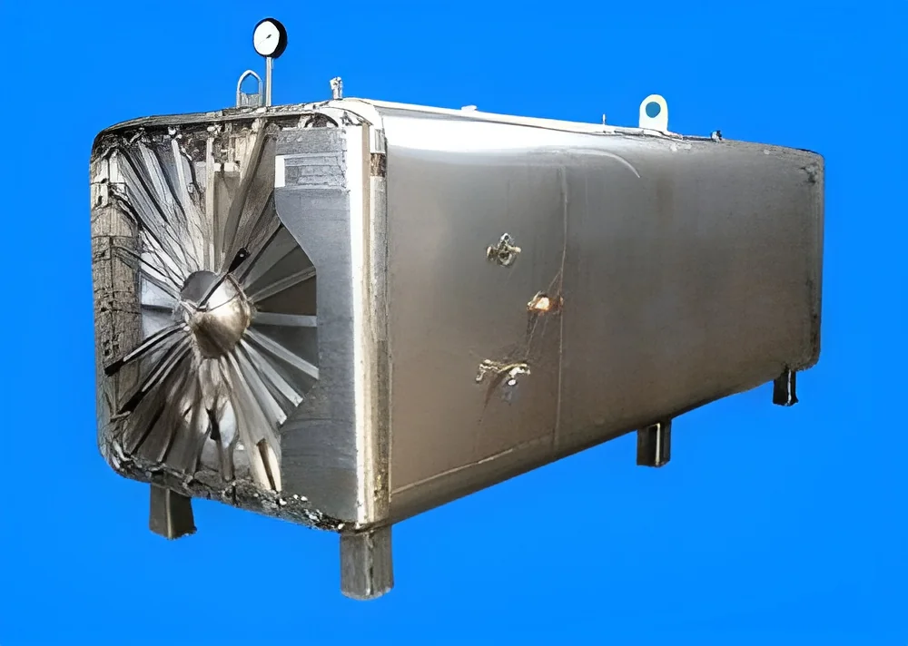
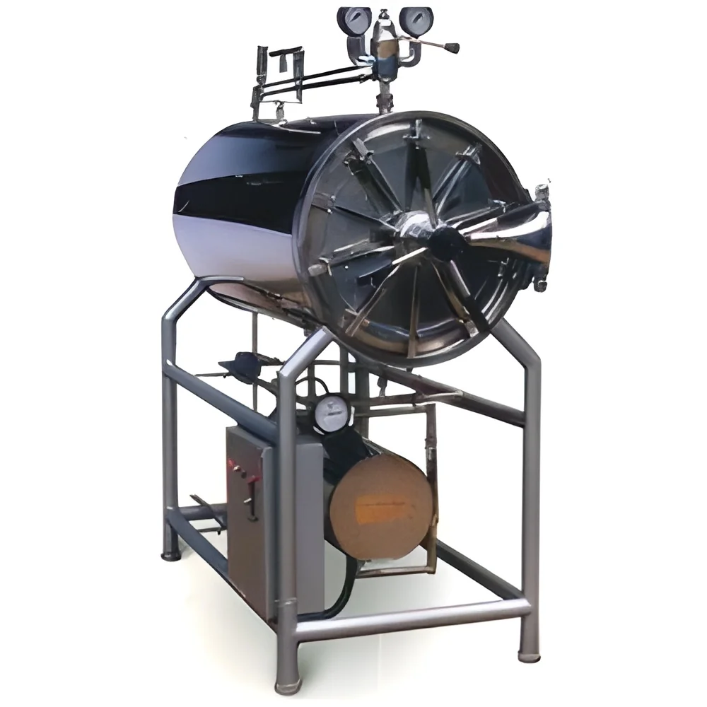
The Molecular Beam Epitaxy Vacuum Chamber represents advanced technology designed specifically for ultra-high vacuum operations at 10⁻⁸ Pa. This precision instrument controls deposition rates below 3000 nm per hour, enabling exceptional epitaxial film growth without carrier gas contamination. The system's engineering focuses on maintaining consistent vacuum integrity and deposition accuracy, ensuring researchers and manufacturers achieve reproducible results. Its robust construction and advanced monitoring systems provide reliable performance for critical thin-film applications where purity and precision are essential requirements for successful material development.

This vacuum chamber serves multiple high-technology industries including semiconductor manufacturing, optoelectronics, and renewable energy research. Semiconductor foundries utilize it for developing advanced integrated circuits and quantum computing components. Research institutions employ the system for materials scienc...
The Molecular Beam Epitaxy Vacuum Chamber represents advanced technology designed specifically for ultra-high vacuum operations at 10⁻⁸ Pa. This precision instrument controls deposition rates below 3000 nm per hour, enabling exceptional epitaxial film growth without carrier gas contamination. The system's engineering focuses on maintaining consistent vacuum integrity and deposition accuracy, ensuring researchers and manufacturers achieve reproducible results. Its robust construction and advanced monitoring systems provide reliable performance for critical thin-film applications where purity and precision are essential requirements for successful material development.

This vacuum chamber serves multiple high-technology industries including semiconductor manufacturing, optoelectronics, and renewable energy research. Semiconductor foundries utilize it for developing advanced integrated circuits and quantum computing components. Research institutions employ the system for materials science studies and novel compound development. The aerospace sector benefits from its ability to create specialized coatings and advanced materials. Electronics manufacturers rely on its precision for producing optoelectronic devices, while solar energy researchers use it for developing next-generation photovoltaic materials.

The business value of this vacuum chamber lies in its reliability and consistent performance. Organizations investing in this system gain competitive advantage through superior material quality and research capabilities. The chamber's design ensures minimal downtime and maintenance requirements, reducing operational costs while maximizing research and production output. The proven track record of reliability makes it a trusted choice for critical operations where system performance directly impacts research outcomes and production efficiency.

Key Features:
- Ultra-high vacuum capability maintaining 10⁻⁸ Pa environment
- Controlled deposition rates under 3000 nm per hour
- Carrier gas-free operation ensuring maximum purity
- Advanced monitoring and control systems for precision operation
- Robust construction for reliable long-term performance

Benefits:
- Ensures high-purity thin film deposition without contamination
- Provides precise thickness control for reproducible results
- Reduces operational costs through minimal maintenance requirements
- Enhances research capabilities with reliable system performance
- Supports advanced material development across multiple industries
Specifications
| Additional Information | |
|---|---|
| Country of Origin | India |
Application
The Molecular Beam Epitaxy Vacuum Chamber enables precise thin film deposition in ultra-high vacuum environments (10⁻⁸ Pa) with controlled rates under 3000 nm/hour. This system ensures high-purity crystalline growth without carrier gas contamination, making it essential for advanced material research where exceptional film quality and precise thickness control are critical for successful outcomes across various high-technology sectors.
This precision chamber serves semiconductor manufacturers, research institutions, and electronics developers requiring reliable epitaxial growth capabilities. The system maintains consistent performance and reliability for both production environments and laboratory settings where material purity is non-negotiable. Industries benefit from its ability to produce reproducible results for critical applications in electronics, energy, and advanced materials development.
- Semiconductor wafer manufacturing for integrated circuits
- Optoelectronic device development including LEDs and laser diodes
- Quantum computing component fabrication
- Solar cell research and thin-film photovoltaic development
- Advanced materials research for aerospace applications
Trade Details
| Available Stock | In Stock |
| Sample Availability | No |
Payment Terms
| Payment Terms |
|
Company Profile
J B Engineering, Gujarat
 Gujarat, India
Gujarat, IndiaIndustrial Equipment & Machinery•Manufacturer•Distributor / Wholesaler•Importer / Exporter
Factory Details
Factory SizeBelow 1000 sqm
Annual Production Capacity0
Molecular Beam Epitaxy Vacuum Chamber For Semiconductor Research
Molecular Beam Epitaxy Vacuum Chamber delivers ultra-high vacuum precision (10⁻⁸ Pa) with controlled deposition under 3000 nm/hour for semiconductor research and thin film development applications.
Min. Order Quantity: 1 unit
Shipping
Shipping fee and delivery date to be negotiated. Contact supplier now for more details.
J B Engineering
 Gujarat, India
Gujarat, IndiaIndustrial Equipment & MachineryManufacturer