Kaynes Technology India (P) Ltd

- Products
- Engineering PCB Design
Product Range
Fact Sheet
- Location:Karnataka, India
- Year of Establishment:1988
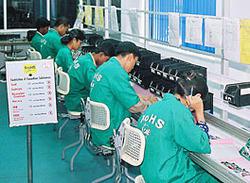
- Business Type:Manufacturer
- Main Products:TURNKEY ELECTRONIC MANUFACTURING SOLUTIONS,Box Build Integratio
- Reviews & Rating:

Get Verified, Sell more with
- Buyer's trust
- Faster conversions
- Better Rankings
- More
Its Free
Verify NowEngineering PCB Design
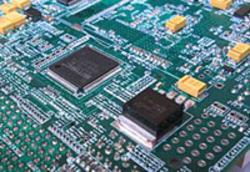
KAYNES recognises customer demands and provides value-added services in design & engineering. KAYNES Technology provides PCB design layout services, generating Gerber data & output files required for manufacturing bare boards.
- FOB PriceNA
- Min Order Quantity50-Pieces
- Payment TermsNA

Product Details
designs with 0.5 mm pitch.
GPS/GSM designsmicroprocessors
I/O interface and industry automationDFM/DFT/DFS review
ESS/EMI/EMS/HALT/HASS
Other Details
KAYNES recognises customer demands and provides value-added services in design & engineering. KAYNES Technology provides PCB design layout services, generating Gerber data & output files required for manufacturing bare boards. We use hi- tech tools like Cadence, PCAD, & CAD star to suit requirements of different customers. Expertise is built-up for designing multilayer PCB with 4 mil trace/ width, build & buried vias and BGA footprint designs with 0.5 mm pitch. Design capabilities exist for RF designs with impedance control and signal integrity checks.
KAYNES provides customized designs for products based on GPS/GSM designs, microprocessors, I/O interface and industry automation/ controls etc.
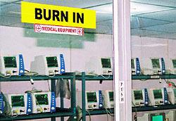
Value-added engineering services support is effective with a strong technical team responsible for process definition, DFM/DFT/DFS review and support for ESS/EMI/EMS/HALT/HASS testing of products.
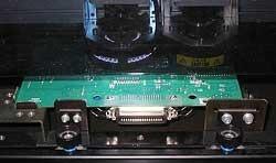
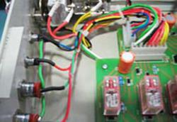
Design support services are offered with area of component re-engineering for obsolescence, up gradation of designs, reliability engineering/ ruggedisation of products to sustain extreme environment conditions.
Images