Jupiter Design Technologies Pvt Ltd

- Products
- PCB-Layout
- PCB Layout
Product Range
Fact Sheet
- Location:Karnataka, India
- Year of Establishment:2002
- Business Type:Manufacturer
- Turnover:Rs. 50 Lakh - 5 Crore
(or USD 100 K - 1 Million) - Main Products: Electronic Boards, Signal Board
- Reviews & Rating:

Get Verified, Sell more with
- Buyer's trust
- Faster conversions
- Better Rankings
- More
Its Free
Verify NowPCB Layout
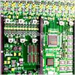
Leveraging on our tools such as Orcad, Cadence & Zuken’s with design capabilities of RF/HF, D/S & Mmulti layer, rigid & flex rigid PCBs, IPC & MIL standards, EMI/EMC & signal integrity verification, RC.
- FOB PriceNA
- Min Order QuantityNA
- Payment TermsNA

Other Details
Leveraging on our tools such as Orcad, Cadence & Zuken’s with design capabilities of RF/HF, D/S & Mmulti layer, rigid & flex rigid PCBs, IPC & MIL standards, EMI/EMC & signal integrity verification, RC and reverse engineering of PCBs we are able to design and develop PCB layouts for various applications across different industries. Our technologies including analog & digital high speed designs, analog switching mode, BGA, through hole & mixed layout, buried, blind & micro via, split power plane, differential pairs, shielded & matched lines, intelligent copper pouring (polygon), guard banding and control impedance are widely used in space, aircraft and defense laboratories.
Images